Technology
Sub Navigation
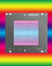
Reticle and Photomasks
Reticles and Photomasks are key elements in the manufacture of integrated circuits, displays, disks, optical networking components, biochips and many other applications. Reticles and photomasks are high precision quartz plates that contain microscopic images of electronic digitized patterns. Enabling the microlithography processes employed in these many applications, reticles and photomasks are used to print critical patterns onto wafers or other substrates in the fabrication of devices.
Photomasks are an integral component in the lithographic process of semiconductor manufacturing. High-purity quartz or glass plates containing precision images of integrated circuits (or chips), photomasks are used as masters by chipmakers, and other industries, to optically transfer these images onto semiconductor wafers. Current advanced lithographic tools, such as deepUV steppers, project light through a photomask and a high aperture lens. The intensity of the light casts an image of the device's design--the pattern on the photomask--onto a silicon wafer coated with a light sensitive material called photoresist. Using negative photoresist the unexposed, or masked, portion of this material is then removed so it can either be etched to form channels or be deposited with other materials. (The process is reversed using positive photoresist.)
Chips are manufactured layer by layer, so these selective deposition/removal steps are repeated until circuit is built. The current generation of semiconductors has many layers, each requiring an unique photomask.
Why is a photomask more than a mere stencil that maps out the chip's design for projecting onto wafers? Because the physical constraints of current lightsources and shrinking design rules driven by the (nearly insatiable) demand for more powerful, faster, lighter and cheaper devices, have rendered the photomask a critical and enabling technology in optical lithography.
Photomasks, requiring sophisticated manufacturing techniques and complex mathematical algorithms to design, are at the forefront of the microminiaturization of chips, enabling more functionality to be embedded within a smaller area. This trend in making devices as powerful and as small as possible facilitates the proliferation of handheld and other portable electronic applications. Although photomasks have always been a necessary component in the chipmaking process, today they are a true enabler of semiconductor technology.